With the rapid advancement of artificial intelligence—particularly generative AI, large language models, and the escalating demand for data center computing—the semiconductor industry is entering a new phase of expansion. AI chips now require greater computing power, energy efficiency, and transistor density, prompting wafer fabs to continually upgrade their manufacturing processes and boost investments in advanced semiconductor equipment.
In the AI era, competition extends beyond chip design to encompass manufacturing capabilities and supply chain collaboration. Lithography systems, etching tools, thin-film deposition equipment, and inspection devices collectively determine whether advanced chips can be produced at scale. Industry leaders such as ASML are emerging as foundational pillars of AI infrastructure.
Why Is AI Driving Continuous Capital Expansion in Wafer Fabs?
Artificial intelligence is fundamentally reshaping semiconductor demand. Previously, growth in the chip market was fueled by smartphones, PCs, and consumer electronics. Now, AI is the new growth engine. Training large AI models, providing inference services, and supporting cloud computing all require vast numbers of high-performance GPUs, AI accelerators, and server chips.
These chips share a defining characteristic: extreme manufacturing complexity. To maximize AI computing efficiency, chipmakers must pack more transistors into limited space while minimizing energy consumption. Advanced process nodes have therefore become essential to boosting chip performance.
For instance, cutting-edge GPUs and AI accelerators require the latest manufacturing nodes, compelling wafer fabs to deploy more precise production equipment. As a result, leading global foundries are ramping up capital expenditures to build new advanced process lines and expand capacity.
TSMC continues to invest in advanced process and packaging technologies to meet surging AI chip demand; Samsung Electronics is expanding its footprint in advanced logic and memory; Intel is enhancing its position in advanced processes through its wafer manufacturing strategy.
These investments ultimately translate into greater demand for semiconductor equipment. Building an advanced process line requires massive equipment outlays, with lithography tools typically representing the most valuable and technically challenging segment.
Thus, the rise of AI is not only fueling chip demand but also accelerating the upgrade of the entire semiconductor equipment industry.
ASML’s Role in the AI Chip Supply Chain
ASML does not design or manufacture AI chips directly; instead, it provides the critical equipment needed for their production.
The chip supply chain typically includes:
- Chip design
- Semiconductor manufacturing
- Packaging and testing
- End-user applications
Wafer manufacturing is the vital bridge between design and finished chips, and lithography technology determines the limits of chip production precision.
ASML’s value lies in its advanced lithography capabilities. Today, EUV lithography systems are indispensable for advanced logic chip production. Using 13.5 nm extreme ultraviolet light, these machines precisely transfer complex circuit patterns onto wafers, enabling the fabrication of smaller, denser transistor structures.
For AI chips, greater transistor density equates to higher computational power. High-end GPUs and AI accelerators require massive numbers of compute units, and advanced manufacturing enables chip designers to integrate more functions into the same footprint.
In this way, ASML serves as a foundational infrastructure provider for the AI chip supply chain. While attention often focuses on chip design firms, without advanced manufacturing equipment, chip designs cannot be mass-produced.
This is why ASML’s strategic value in the semiconductor ecosystem continues to climb.
How Lithography Machines Shape Advanced Logic Chips and HBM
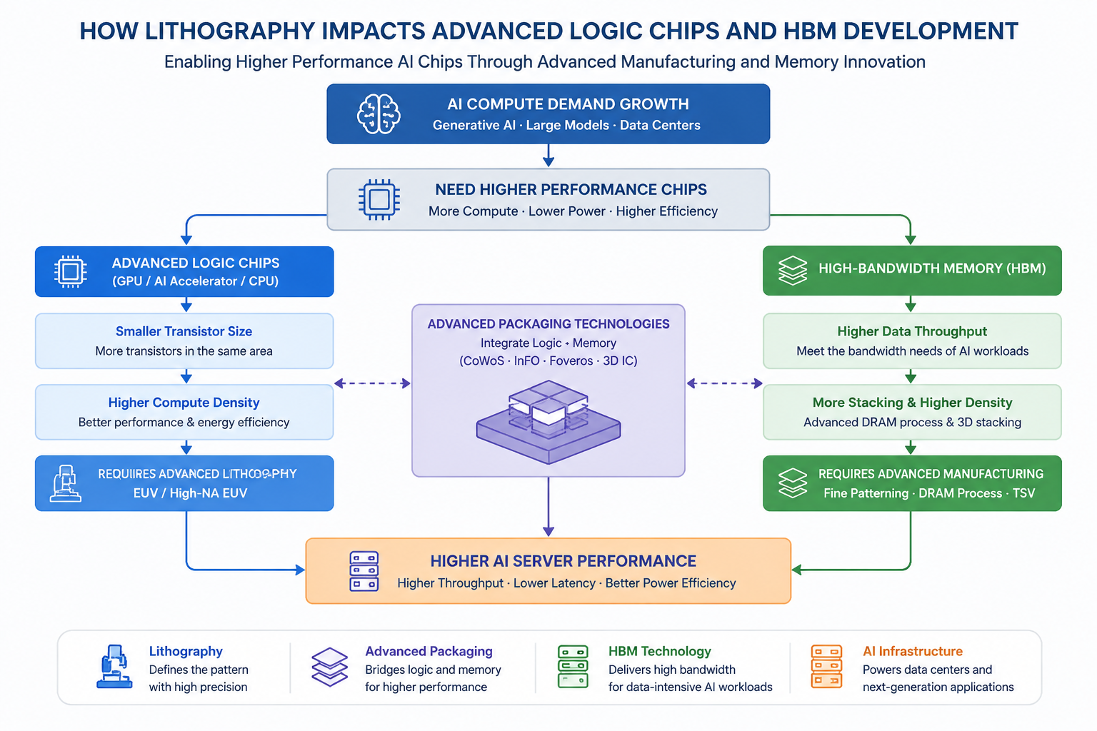
AI chip innovation depends not only on logic chip manufacturing but also on high-bandwidth memory (HBM). HBM is a crucial element of AI accelerators, delivering higher data throughput to meet the memory bandwidth needs of large-scale AI model training.
HBM production also demands advanced semiconductor processes. For logic chips, advanced lithography determines the performance of compute cores; for memory, high-precision manufacturing impacts chip stacking, interconnects, and yield.
The evolution of AI chips is driving the convergence of “advanced logic + high-performance memory + advanced packaging.” Modern AI GPUs are no longer single chips—they integrate compute cores, HBM, and advanced packaging into complete systems.
In this context, lithography equipment becomes even more critical. Next-generation processes allow chipmakers to reduce power consumption, boost compute efficiency, and enable more complex designs. ASML’s technology thus impacts not only CPUs, GPUs, and other logic chips, but also indirectly enhances the performance of entire AI server systems.
Why AI Infrastructure Fuels Semiconductor Equipment Demand
The buildout of AI infrastructure is creating a new demand cycle for semiconductors.
Data centers require massive numbers of servers, GPUs, networking hardware, and storage systems to support AI model training.
All of this infrastructure relies on semiconductors.
Compared to traditional internet services, AI workloads demand more chips and higher performance, prompting cloud providers to expand their data center investments.
As data centers scale up, upstream chip manufacturing demand rises in parallel.
To keep pace, wafer fabs must expand capacity and upgrade manufacturing technologies.
This drives greater adoption of lithography, etching, and inspection equipment.
Beyond ASML, the entire semiconductor equipment supply chain is being propelled by AI trends.
For example:
- Lithography equipment determines patterning precision
- Etching equipment forms microscopic structures
- Deposition equipment creates thin-film layers
- Inspection equipment ensures manufacturing yield
As AI chips become more complex, the technical requirements for all these systems increase.
Thus, AI is not only fueling the growth of chip companies but also driving upgrades across the semiconductor manufacturing ecosystem.
How ASML, Applied Materials, Lam Research, and KLA Collaborate in the Industry Chain
Semiconductor manufacturing is a complex, multi-step process—not the result of a single tool or company. While ASML leads in advanced lithography, chip production also depends on other major equipment manufacturers.
In the AI chip era, the need for advanced process nodes and high-performance computing is pushing the entire semiconductor equipment supply chain to upgrade. Different equipment vendors are responsible for critical steps in wafer fabrication, collectively shaping the chip’s final performance, cost, and yield.
Key players include ASML, Applied Materials, Lam Research, and KLA.
Applied Materials specializes in thin-film deposition, materials engineering, and related tools. Chip manufacturing requires the formation of multiple complex layers on wafers, and deposition technology determines the accuracy and stability of these layers.
Lam Research focuses on etching and cleaning equipment. As chips become more three-dimensional, precise etching is essential for forming microscopic circuits and transistor structures, making etching technology increasingly crucial.
KLA provides semiconductor inspection and metrology equipment. As manufacturing enters the nanometer era, even minute defects can impact yield, making inspection technology vital for boosting fab productivity.
- In the manufacturing process:
- Lithography defines the pattern
- Deposition builds material layers
- Etching forms structures
- Inspection detects problems
These steps are interdependent, collectively forming the advanced chip manufacturing ecosystem.
AI chips require greater manufacturing precision, driving not only demand for ASML’s EUV systems but also upgrades across the semiconductor equipment sector.
Looking ahead, as advanced process nodes continue to evolve, collaboration among equipment vendors is likely to deepen. Competition in chip manufacturing is shifting from individual technologies to the strength of the entire semiconductor ecosystem.
Opportunities and Challenges in the Semiconductor Equipment Industry
The AI boom presents new growth opportunities for semiconductor equipment makers, but the industry still faces significant challenges.
AI Demand Spurs Equipment Investment
Generative AI, large-scale model training, and intelligent computing are driving sustained global demand for high-performance chips. To meet this demand, wafer fabs must expand advanced process capacity, increasing equipment purchases.
For advanced equipment providers like ASML, long-term technology trends remain highly supportive.
Continuous Innovation in Advanced Manufacturing
As process nodes shrink, manufacturing complexity rises.
Historically, the industry improved performance mainly through transistor scaling, but future progress will depend on advanced packaging, chiplets, 3D integration, and new materials.
These innovations create new equipment needs.
However, the industry faces several challenges:
-
High cyclicality.
Semiconductor equipment sales are closely tied to fab capital expenditures. When chip demand is strong, fabs invest more; when supply and demand are out of balance, equipment spending falls.
Even industry leaders like ASML are affected by these cycles.
-
Rising R&D costs.
Developing advanced equipment requires sustained investment in materials research, engineering validation, and production optimization.
Next-generation technologies such as High-NA EUV involve even greater complexity and expense.
-
Global supply chain and policy uncertainties.
Semiconductor equipment is now a focal point in global technology competition, and export policies for advanced manufacturing tools can affect market strategies.
Companies must maintain technical leadership while adapting to global industry shifts.
How Global Fab Expansion Impacts ASML
The global expansion of wafer fabs is a key driver of ASML’s long-term growth. As demand for AI, automotive electronics, cloud computing, and smart devices rises, regions worldwide are investing in semiconductor manufacturing.
Asia continues to lead in advanced manufacturing, with TSMC expanding its process and packaging capabilities to serve AI chip clients.
Meanwhile, the US, Europe, Japan, and others are promoting domestic fab investments to mitigate supply chain risks. All new fabs require substantial equipment purchases. For ASML, advanced fab expansion means increased demand for EUV and DUV systems—especially for advanced logic chips, where EUV is now indispensable.
Fab expansion also drives equipment upgrade demand. Given the high cost of lithography tools, fabs typically upgrade existing systems as well as buy new ones, boosting productivity and manufacturing capability. This creates a long-term revenue stream for ASML’s service business.
Additionally, as AI chip demand grows, advanced packaging and memory are also expanding rapidly. While these segments do not rely exclusively on EUV, overall semiconductor investment growth increases equipment industry scale. Thus, global fab expansion benefits ASML and the entire semiconductor equipment ecosystem.
The Future of AI Semiconductor Equipment
The future of AI semiconductor equipment will focus on higher precision, greater efficiency, and intelligent manufacturing.
- Ongoing innovation in advanced lithography.
High-NA EUV is emerging as the next leap beyond EUV.
By increasing numerical aperture, High-NA EUV delivers higher lithography resolution, supporting even more advanced chip nodes.
While this technology is costlier and more complex, the relentless demand for AI computing power will only heighten the importance of advanced manufacturing.
- Intelligent semiconductor manufacturing.
As chip designs grow more complex, traditional manual methods are no longer sufficient.
Future fabs will increasingly deploy AI-assisted manufacturing, using machine learning to optimize production parameters, boost equipment utilization, and improve yield.
This demands greater data analytics capabilities from semiconductor equipment itself.
-
Rising demand for advanced packaging equipment.
As transistor scaling becomes more challenging, the industry is turning to multi-chip combinations for performance gains. Chiplets, 3D packaging, and HBM stacking are becoming central to AI chip innovation. The scope of equipment competition will extend from wafer fabrication to packaging and testing.
-
More pronounced equipment ecosystem competition.
Next-generation chip manufacturing will require coordinated optimization across lithography, etching, deposition, inspection, packaging, and more.
While individual equipment advantages remain important, ecosystem-level manufacturing capabilities will define future competitiveness.
Conclusion
AI semiconductors are driving a new upgrade cycle in global chip manufacturing, with semiconductor equipment as the critical infrastructure supporting this transformation. ASML, with its EUV lithography technology, occupies a central position in advanced chip production. As demand for AI chips, high-performance computing, and data centers continues to surge, fabs are ramping up capital expenditures, further increasing the need for advanced lithography systems.
However, the evolution of the AI semiconductor sector is not the work of a single company. ASML, Applied Materials, Lam Research, KLA, and other equipment providers each play vital roles in lithography, deposition, etching, and inspection, together forming the backbone of modern chip manufacturing.
Looking forward, as demand for AI computing power grows, advanced process nodes progress, and technologies like High-NA EUV and advanced packaging mature, the semiconductor equipment industry is poised for long-term growth. At the same time, the industry must contend with cyclical trends, R&D costs, supply chain realignment, and shifting global policies.
Ultimately, competition in the AI era is not just about models and applications—it’s about manufacturing prowess. Semiconductor equipment companies are emerging as the driving force behind this new wave of technological innovation.