Lumentum is a company specializing in optical communications and photonics, with core operations spanning lasers, optical components, and high-speed communication solutions. As AI infrastructure rapidly evolves, Lumentum leverages its expertise in optical devices to participate in the CPO, silicon photonics, and high-speed optical interconnect supply chain—delivering key components for next-generation data center connectivity.
The advancement of CPO is crucial not only for unlocking AI chip performance, but also for shaping the future architecture of data center networks. As demand for 800G and 1.6T optical communications rises and AI clusters scale up, optical interconnect technology is shifting from an auxiliary solution to a foundational element of AI infrastructure.
What Is CPO (Co-Packaged Optics)
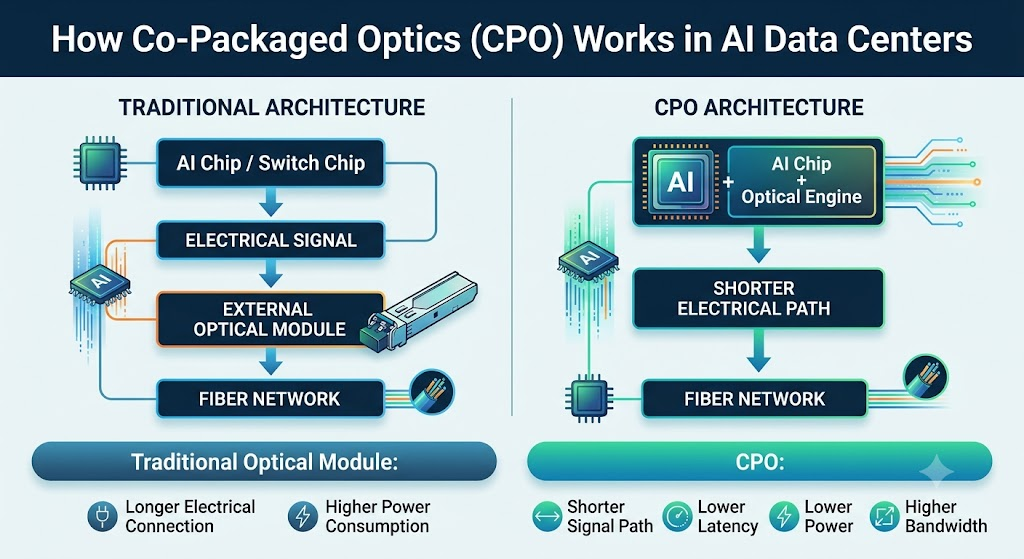
CPO (Co-Packaged Optics) is an advanced interconnect technology that integrates optical devices and core chips within a single system. Its goal is to minimize the data transmission distance between chips and optical modules, thereby boosting high-speed communication efficiency. Traditional data center networks typically use a discrete optical module architecture: chips inside servers or switches handle data processing, while external optical modules connect via electrical interfaces, converting signals between electrical and optical domains.
This architecture has fueled the growth of the internet and cloud computing for decades. However, as AI data centers expand rapidly, the traditional model is encountering new challenges.
AI training tasks require extensive GPU collaboration, with data exchange volumes between GPU clusters far exceeding those of traditional applications. Supporting large-scale AI model training necessitates more high-speed switching chips and network connectivity. As transmission speeds increase, high-speed electrical connections between chips and optical modules lead to greater signal loss and power consumption. At the 800G and 1.6T communication thresholds, traditional architectures face signal attenuation, thermal management challenges, and declining energy efficiency.
CPO fundamentally rethinks this connection paradigm. By positioning the optical engine adjacent to the switching chip, CPO shortens the high-speed electrical signal path, reduces signal loss, and lowers system power consumption—making it a pivotal technology for next-generation AI data center networks.
Major chipmakers, network equipment vendors, and optical communications firms are actively pursuing CPO technology.
Key Differences Between CPO and Traditional Optical Modules
The primary distinction between CPO and traditional optical modules lies in how optical components interface with the chip.
Traditional optical module architecture: chip → electrical interface → optical module → optical fiber
CPO architecture: chip + optical engine → direct optical fiber connection
In traditional setups, chip-generated data is first converted into high-speed electrical signals, then sent to an external optical module for electro-optical conversion. As speeds escalate, this electrical path becomes a performance bottleneck. CPO improves conversion efficiency by bringing the optical interface closer to the chip.
Key differentiators include:
-
Power consumption: Energy use is a major cost driver in AI data centers. As GPU counts rise, so does network power draw. CPO's shorter high-speed electrical links help reduce communications-related energy consumption.
-
Bandwidth: Future AI clusters demand ultra-high-speed data exchange. While traditional optical modules continue to evolve, higher rates increase system complexity. CPO provides an architecture better suited to high-bandwidth environments.
-
System design: Traditional optical modules offer strong modularity for easy maintenance and replacement. CPO, by contrast, emphasizes co-design across chips, packaging, and optics, raising the bar for manufacturing capabilities.
CPO is not a simple replacement for legacy optical modules—it’s a new technical path for high-performance AI compute scenarios.
Why AI Chips Are Accelerating CPO Adoption
The relentless performance gains of AI chips are a major driver of CPO interest. Modern AI accelerators deliver ever-increasing compute, with each GPU or AI chip handling larger datasets. To maximize this performance, multiple compute nodes must be linked over high-speed networks.
In large-scale AI data centers, compute tasks are distributed across vast GPU clusters. For example, training a large language model may require thousands of GPUs simultaneously exchanging model parameters and results.
This demands network connectivity that keeps pace. If network speeds lag, even the most powerful GPUs can be underutilized due to data transfer delays. Traditional electronic interconnects face growing challenges at high speeds:
-
Shortened high-speed signal distances
-
Increased power consumption
-
More demanding thermal management
As a result, the AI industry is seeking new interconnect paradigms. CPO’s value lies in breaking traditional connectivity bottlenecks, enabling more efficient data exchange between high-speed chips.
As AI inference workloads grow, data centers must not only train large models but also process massive user requests in real time—raising the bar for low-latency, high-bandwidth networks.
Lumentum’s Strategy for Next-Generation Optical Interconnects
Lumentum (LITE) is a global leader in optical communications and laser technology, with core strengths in photonic devices, lasers, and high-speed communications components. Within the CPO supply chain, Lumentum does not manufacture AI chips directly; instead, it provides the critical optical components required for high-speed optical connectivity.
While CPO architectures reduce the distance between chips and optical modules, they still rely on high-performance light sources, optical engines, and advanced optical devices.
Lasers are a particularly vital element, directly impacting optical communications performance. High-speed AI networks require stable, high-speed modulated optical signals, with lasers determining signal quality, transmission speed, and overall system reliability. Lumentum’s deep expertise in photonics positions it to play a key role in high-speed optical interconnect markets.
As AI data centers migrate to higher speeds, demand is surging for:
These areas align closely with Lumentum’s technical focus. As CPO commercialization accelerates, the importance of optical device suppliers will only grow—regardless of data center architecture, high-performance optical components are foundational for high-speed connectivity.
Synergy Between Silicon Photonics and CPO
Silicon photonics is a foundational enabler for CPO. Simply put, silicon photonics leverages mature semiconductor manufacturing to integrate optical devices onto silicon chip platforms.
Whereas traditional optical communications depend on discrete optical components, silicon photonics seeks to achieve higher integration—lowering costs and boosting performance.
CPO and silicon photonics are highly synergistic:
Combined, they further enhance data center network transmission efficiency.
For AI data centers, this synergy is critical.
As AI chip performance soars, data transfer speeds must keep pace. Relying on numerous discrete optical modules increases system complexity and power consumption.
Silicon photonics reduces the size of optical components and improves manufacturing efficiency, while CPO shortens the distance between chips and optical modules. Together, they drive the evolution of next-generation high-speed interconnect architectures.
Major global semiconductor and optical communications companies are advancing research in both silicon photonics and CPO.
Lumentum has a strong technical foundation here, with longstanding R&D in lasers and photonic devices. Light sources, modulators, and optical components are all essential to silicon photonics and CPO systems.
As CPO transitions from lab validation to widespread deployment, companies with deep photonics expertise are poised to capitalize on new industry opportunities.
CPO’s rise as a core AI infrastructure technology has drawn in a range of supply chain leaders—most notably Lumentum, Broadcom, and Marvell, each with distinct technical positioning.
Lumentum is fundamentally an optical communications device supplier.
Its core strengths are in lasers, optical components, and photonic technology. Within CPO architectures, Lumentum focuses on light sources and optical components, providing the foundational devices for high-speed data transfer.
Broadcom Inc. is more system-level infrastructure-focused.
Broadcom is a key player in data center switching chips, and it is also active in network ASICs, connectivity chips, and AI infrastructure solutions. In CPO, Broadcom’s edge comes from its chip and network system capabilities.
For example, AI data centers require high-speed switching chips to manage traffic between massive GPU clusters—an area where Broadcom excels.
Marvell Technology, Inc. is primarily focused on data center connectivity, network chips, and optoelectronic conversion technologies.
Marvell has strong positions in high-speed interconnects, including data center networks, storage connectivity, and optical communications chips.
In summary:
-
Lumentum: optical devices and laser technology
-
Broadcom: network chips and system platforms
-
Marvell: connectivity chips and data infrastructure
CPO commercialization is not driven by a single company—it requires coordinated advances across chips, packaging, optics, and networking equipment.
Commercialization Challenges for CPO
While CPO is widely seen as the future of AI optical interconnects, several hurdles remain before mass adoption.
Manufacturing complexity: Traditional optical modules are highly modular, allowing for easy replacement of faulty components. CPO’s high integration of optics and chips makes manufacturing and maintenance more challenging.
This demands advanced packaging, testing, and supply chain collaboration capabilities.
Industry standards: The data center ecosystem spans chipmakers, server vendors, network equipment manufacturers, and cloud providers. There are still divergent requirements for CPO architectures, interface standards, and application methods.
Unified industry standards are essential for scaling CPO deployment.
Cost: While CPO promises lower long-term operating power consumption, initial R&D and manufacturing costs are high. For major cloud players, technology advantages must translate into investment returns.
If CPO device costs fall too slowly, legacy optical modules may persist in select markets.
Thermal management and reliability: As device density increases in AI data centers and chips and optics are placed in closer proximity, ensuring long-term stability requires new engineering solutions.
Thus, CPO’s evolution is not a simple swap for existing technology, but a gradual, stepwise process.
The Future of Next-Generation AI Optical Interconnects
The evolution of AI optical interconnect technology will center on three pillars: higher speeds, lower power consumption, and deeper integration.
-
Speed upgrades: Data centers are moving from 400G to 800G optical communications, and as AI clusters grow, 1.6T and beyond will be the next milestones. This will drive ongoing innovation in lasers, optical chips, and packaging.
-
Large-scale CPO adoption: CPO is still in the industrialization phase, but as AI chip power and network demands rise, its value proposition is expanding. CPO is likely to debut in hyperscale AI data centers, then spread to broader high-performance computing scenarios.
-
Optical computing and advanced photonics: As AI models increase in complexity, traditional electronic compute architectures may hit limits. Optical computing, silicon photonics, and advanced photonic systems could become vital additions to compute infrastructure. For Lumentum, long-term opportunity lies in industry-wide optical communications upgrades.
AI’s rise is driving not just higher GPU demand but a holistic upgrade of network connectivity, data transfer, and infrastructure technology. Optical interconnects are becoming a cornerstone of the AI ecosystem.
Conclusion
CPO (Co-Packaged Optics) is emerging as a key next-generation high-speed interconnect technology for AI data centers. As AI models scale, massive GPU clusters require ever-higher bandwidth and lower latency, exposing the power and performance limits of traditional optical module architectures. By tightly integrating optical components and chips, CPO reduces high-speed signal transmission distances and boosts network efficiency. Meanwhile, advances in silicon photonics are accelerating optical system integration, laying the groundwork for future high-speed AI networks.
Lumentum (LITE), as a leader in optical communications and laser technology, serves primarily as a supplier of optical devices and laser components within the CPO supply chain. While Broadcom leads in network chips and Marvell in connectivity chips, Lumentum is focused on the photonics segment.
Nonetheless, CPO commercialization still faces challenges around manufacturing complexity, cost, standardization, and reliability. As AI data centers continue to expand, the importance of high-speed optical interconnects is set to grow.
From an industry perspective, AI competition is shifting from pure compute to data transmission capabilities. CPO, silicon photonics, and high-speed optical communications will be critical to supporting next-generation AI infrastructure, with optical communications companies like Lumentum playing a pivotal role in this technological evolution.