In today’s semiconductor industry, boosting chip performance depends not only on architectural innovation but also on the sophistication of manufacturing processes. As AI chips, data center GPUs, high-performance computing processors, and smart devices evolve rapidly, manufacturers must pack more transistors into ever-smaller spaces. EUV lithography has emerged as the essential technology enabling this progress.
From an industry chain perspective, EUV lithography marks a pivotal step forward in advanced manufacturing. The ecosystem built around EUV—including equipment, materials, optical systems, and software—has become a strategic asset in the global race for semiconductor leadership. ASML stands at the center of this competition, leveraging its world-class EUV lithography systems to play a critical role in next-generation chip fabrication.
What Is EUV Lithography?
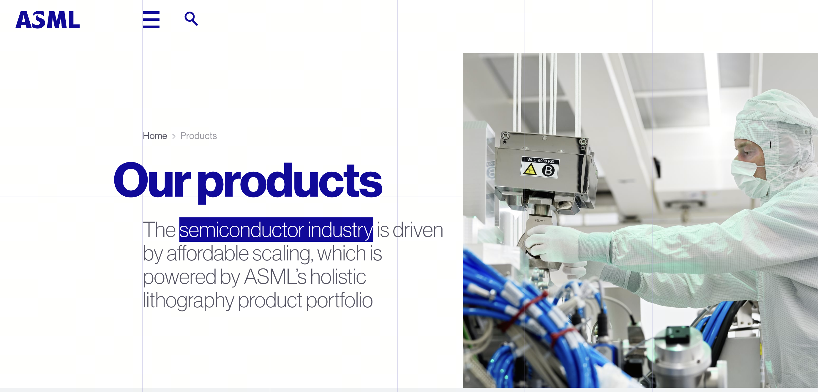
EUV (Extreme Ultraviolet) lithography is a cutting-edge technology that uses extremely short-wavelength light to expose chip patterns. In essence, lithography is “printing” circuit diagrams onto silicon wafers using light. Foundries employ lithography machines to transfer intricate chip designs onto a photoresist layer on the wafer’s surface, which is then processed through etching, deposition, and other steps to form the final chip.
While traditional lithography tools use longer-wavelength ultraviolet light, EUV operates at just 13.5 nm. The shorter the wavelength, the higher the potential resolution, allowing EUV to create much finer chip structures.
Currently, ASML is the world’s sole commercial supplier of EUV lithography machines. Its systems are used by leading foundries including TSMC, Samsung Electronics, and Intel.
EUV lithography systems are engineering marvels—each machine contains tens of thousands of precision components and must deliver extreme optical accuracy, mechanical stability, and operate in high-vacuum conditions.
A core technical challenge lies in generating the EUV light itself. Since 13.5 nm light cannot pass through conventional lenses, EUV systems rely on reflective optics. The light is produced by firing a high-energy laser at tin droplets in a vacuum, creating plasma that emits the EUV light needed for chip patterning.
EUV lithography is not a simple upgrade of traditional technology; it’s a multidisciplinary leap, integrating physics, optical engineering, materials science, and precision manufacturing.
How Does EUV Differ from DUV Lithography?
Before EUV, the industry depended on DUV (Deep Ultraviolet Lithography), which uses 248 nm or 193 nm light sources—most notably, the 193 nm ArF (argon fluoride) systems that powered decades of process advancement.
The main difference is wavelength: DUV uses longer ultraviolet light, while EUV’s 13.5 nm wavelength delivers much higher resolution for finer transistor features.
Technologically, DUV relies on multiple patterning—requiring repeated exposures and overlays—to achieve advanced nodes. This extends DUV’s usefulness but adds steps, increases cost, and impacts yield and throughput. EUV streamlines this by reducing or eliminating many complex multi-patterning flows, making advanced manufacturing more efficient.
However, EUV adoption comes with significant hurdles: extremely high equipment costs, technical complexity, and demanding maintenance. A single advanced EUV system can cost hundreds of millions of dollars, and foundries must make massive investments in supporting infrastructure. As a result, EUV supplements—rather than wholly replaces—DUV. DUV systems remain prevalent for mature nodes, automotive chips, and analog devices.
Why Is EUV Essential for Advanced Nodes?
The goal of advanced process nodes is to fit more transistors into smaller chips. Moore’s Law has long driven the industry by shrinking transistor sizes, but traditional approaches are hitting physical limits.
At 7 nm, 5 nm, and now 3 nm, DUV alone is no longer sufficient. Without EUV, foundries would need even more complex multi-patterning, driving up costs and reducing efficiency.
EUV enables scalable, stable production at the most advanced nodes.
Today’s flagship smartphone processors, AI GPUs, and data center chips all rely on advanced nodes—and, by extension, on advanced lithography. In the AI era, chip requirements have shifted: traditional processors focus on raw performance, while AI chips prioritize parallelism, energy efficiency, and massive data throughput. These needs drive up transistor counts and internal complexity.
Advanced manufacturing processes empower chip designers to boost performance and lower the cost per computation, making EUV lithography a cornerstone of AI infrastructure.
How Does ASML Sustain Its Leadership in Lithography?
ASML’s dominance in EUV is the result of decades of R&D, deep industry collaboration, and a robust global supply chain.
EUV innovation is a marathon.
It took ASML more than ten years to move EUV from concept to commercial reality, solving challenges in light source efficiency, optics, and system stability along the way.
The supply chain is highly specialized and global.
No single company can build an EUV system alone. ASML partners with top suppliers—like ZEISS for optics and others for mechanics, controls, and critical components—creating formidable barriers to entry.
Long-term partnerships with leading foundries.
Because advanced chip manufacturing demands exceptional reliability, foundries are reluctant to switch suppliers. Once ASML is embedded in a customer’s production line, it becomes a long-term partner.
ASML continues to push boundaries with High-NA EUV, targeting even greater resolution for future nodes.
Why Is AI Driving EUV Demand?
The AI boom is reshaping the semiconductor landscape and fueling unprecedented demand for EUV lithography.
Technologies like generative AI, large language models, and high-performance computing require vast computational resources—delivered by advanced GPUs, AI accelerators, and server processors.
These chips demand high transistor density, computational throughput, and energy efficiency—requirements that only advanced process nodes can meet.
As AI chip designs become more complex, the value of advanced lithography grows. Smaller transistors mean more compute units per chip and lower power consumption. This is why top chip designers are racing to adopt the latest nodes and why EUV is indispensable.
The AI chip ecosystem is tightly integrated: design companies innovate architectures, foundries handle manufacturing, and equipment firms like ASML provide the critical tools.
AI’s rise is also driving massive capital investment in new production lines for future AI servers, cloud infrastructure, and data centers. All of this translates to surging demand for advanced semiconductor equipment.
Still, EUV demand is not immune to market cycles—foundry investments depend on global economic conditions, chip supply-demand, and industry trends. Long-term EUV growth is powered by technology, but short-term results will fluctuate with the semiconductor cycle.
How Do ASML, Nikon, and Canon Compare?
ASML, Nikon, and Canon are the leading players in the global lithography market, but their strategies and strengths diverge:
| Dimension |
ASML |
Nikon |
Canon |
| Core Focus |
Lithography market leader |
Lithography & precision optics |
Lithography & imaging optics |
| Key Strengths |
EUV, advanced nodes |
DUV, mature nodes |
DUV, mature nodes, specialty apps |
| EUV Capability |
Commercialized, industry-leading |
No commercial EUV |
No commercial EUV |
| DUV Capability |
High-end DUV & EUV |
Strong DUV, competitive in select markets |
Strong DUV, broad process coverage |
| Main Customers |
Advanced logic, top foundries |
Mature nodes, some IDMs |
Mature nodes, power, MEMS, specialty |
| Technical Barriers |
EUV source, mirrors, system integration |
Precision optics, exposure tech |
Optics, exposure, precision manufacturing |
| Market Position |
Advanced node leader |
Mature/specialty market focus |
Mature/specialty market focus |
| Competitive Edge |
Near-monopoly in advanced EUV |
Strong DUV position |
Strong DUV & specialty process position |
Nikon and Canon have a rich legacy in lithography, especially in DUV and mature nodes. Japanese firms once dominated, but as the market shifted to advanced nodes, EUV became the battleground.
ASML’s advantage is the successful commercialization of EUV—a feat requiring solutions to:
- Light source: EUV cannot be produced by traditional means; stable generation is a complex challenge.
- Optics: EUV’s short wavelength demands ultra-precise mirrors instead of lenses.
- System stability: Advanced foundries require continuous, reliable operation to maintain yield and control costs.
These hurdles have solidified ASML’s lead. While Nikon and Canon excel in optics, they have yet to commercialize EUV at scale.
Today, ASML dominates advanced logic manufacturing, while Nikon and Canon focus on DUV, mature nodes, and specialty applications.
Lithography, though critical, is just one part of the semiconductor equipment ecosystem. Etch, deposition, inspection, and other tools are also essential, but ASML’s strength is concentrated in lithography.
What Are the Challenges Facing EUV Lithography?
Despite its central role in advanced chipmaking, EUV lithography faces several headwinds:
- High equipment costs: EUV systems are extraordinarily expensive and require custom facilities, maintenance, and expert personnel. Only the largest semiconductor companies can afford large-scale deployment.
- Rising technical complexity: As nodes advance, foundries demand even greater precision, speed, and efficiency. ASML is developing High-NA EUV for even finer resolution, but commercializing new technologies takes time and rigorous validation.
- Supply chain risks: The semiconductor industry is now at the heart of global tech competition, and advanced manufacturing equipment is subject to increasing policy scrutiny. EUV tools depend on a global supply chain; any disruption can impact production and delivery.
- Chipmaking is a system: Lithography is vital, but advanced chipmaking involves materials, design, packaging, and production management. Future competition will be ecosystem-based, not just about any single tool.
Where Is Lithography Technology Headed?
Over the next few years, lithography will focus on higher resolution, greater productivity, and lower costs.
High-NA EUV is the most anticipated next step, using a larger numerical aperture for even finer patterning and supporting future nodes.
Compared to current EUV, High-NA systems are more complex and costly. But as demand for AI, HPC, and advanced processors grows, the market is poised to drive these innovations forward.
Software is also becoming a key differentiator. As chip designs grow more complex, improvements in computational lithography, AI-driven optimization, and advanced algorithms are essential for better exposure and yield.
The future is a “hardware + software + data” convergence.
At the same time, the industry is exploring advanced packaging, chiplets, and 3D integration. These won’t replace EUV, but will complement it, further boosting chip performance.
For ASML, growth will come not just from selling more EUV tools, but also from upgrades, software services, and ecosystem development.
As global demand for AI Hashrate accelerates, advanced lithography will remain indispensable.
Conclusion
EUV lithography is one of the most transformative breakthroughs in modern semiconductor manufacturing. With 13.5 nm extreme ultraviolet light, it enables foundries to create smaller, denser, and more powerful chips.
Compared to DUV, EUV is a game-changer for advanced nodes like 7 nm, 5 nm, and 3 nm.
ASML’s long-term investment, global supply chain integration, and leadership in EUV commercialization have made it the linchpin of advanced lithography. As AI, high-performance computing, and data centers surge, the importance of EUV equipment only grows.
Still, the EUV industry faces steep costs, technical complexity, supply chain risks, and the challenge of scaling new technologies. The evolution of High-NA EUV, computational lithography, and smart manufacturing will continue to drive the industry toward greater precision and efficiency.
In the context of global technology, EUV lithography machines are more than just tools—they’re the backbone of the advanced chip era. Understanding EUV is key to understanding the shifting dynamics of global semiconductor competition in the age of AI.