Elon Musk Launches Terafab Project with $20B–$25B Investment to Achieve 1 Terawatt of Annual Computing Power and Develop Space AI Chips
Pushing Computing Beyond Surface Limits
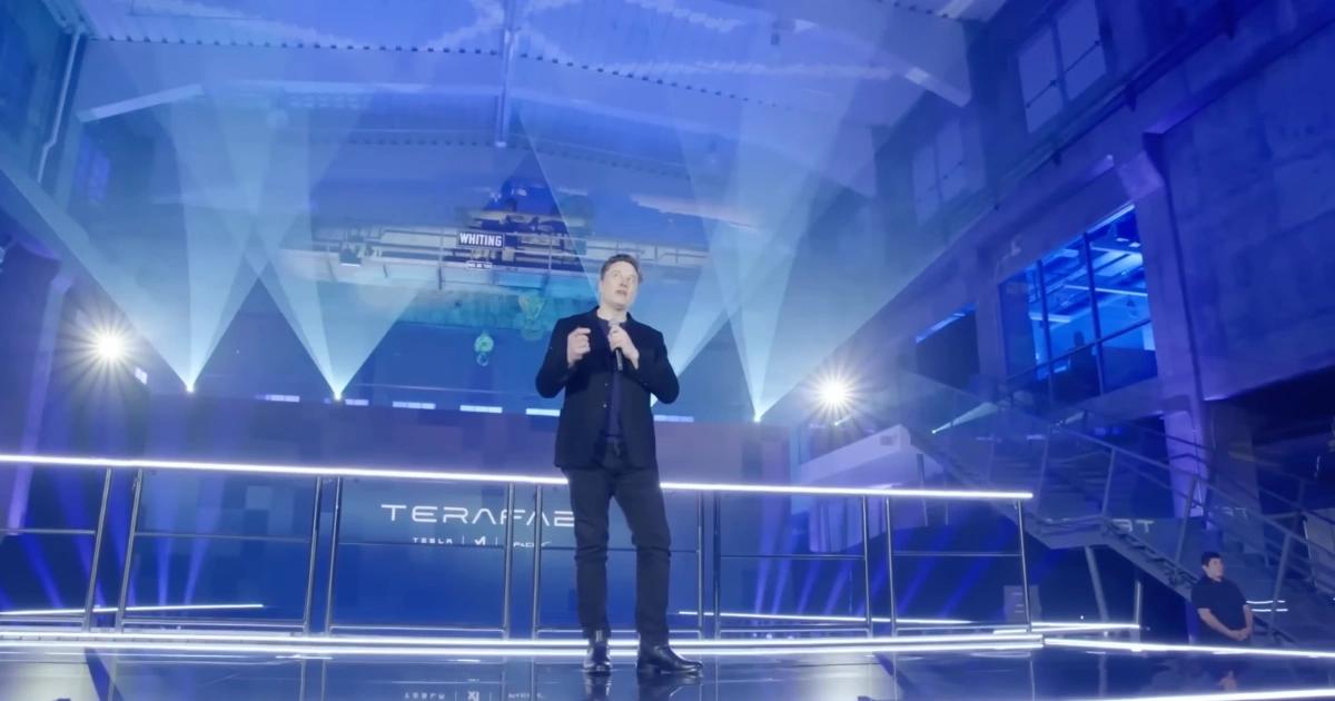
On March 21, Tesla and SpaceX CEO Elon Musk officially announced the “Terafab” semiconductor manufacturing project in Austin, Texas. This massive initiative, estimated to cost between $20 billion and $25 billion, will be operated jointly by Tesla and SpaceX, aiming to produce chips with up to 1 terawatt (TW) of computing capacity annually.
According to Musk, the current global AI computing power is about 20 gigawatts (GW) per year, only 2% of the anticipated future demand. The advanced wafer factory near Austin will have a capacity set to 50 times that of existing semiconductor fabs worldwide.
Musk openly states that, while he appreciates suppliers like TSMC, Samsung, and Micron, their current capacity expansion speeds cannot keep up with his expansion plans. This ambitious project is designed to support the growing needs of robotics, autonomous systems, and space infrastructure, pushing humanity toward galactic civilization.
Vertical Integration and Rapid Manufacturing Revolution
Terafab’s operational model will revolutionize the traditional semiconductor industry’s division of labor by adopting an integrated, end-to-end manufacturing process. The facility will include two independent wafer fabs, each dedicated to a single chip design to streamline processes and boost capacity. Inside, design, fabrication, testing, packaging, and even mask-making will be integrated within the same building. This creates a rapid feedback loop, reducing the cycle from design to testing to under 7 days.
Compared to the industry’s current conservative and rigid practices, Terafab allows for more high-risk, high-reward innovation. Musk plans to redesign any equipment that causes bottlenecks and enable wafer transfer in a linear fashion between adjacent machines to achieve extreme production scale. This transformation grants Tesla and SpaceX greater supply chain autonomy, reducing reliance on external foundries and strengthening their bargaining power in the market.
Orbit AI Satellites: Sending Computing Power into Space
Beyond terrestrial applications, Musk revealed a forward-looking space computing vision. He plans to deploy up to 80% of the chips’ computing power in Earth orbit, leaving only 100–200 GW on the ground. The main reason is that terrestrial power grids cannot handle the massive energy consumption of 1 TW-level computing, whereas space-based solar radiation is about five times that of Earth’s surface, and heat dissipation in vacuum environments is more feasible.
To this end, Terafab will produce two main types of chips: one optimized for edge computing on Earth, such as AI5 or AI6 chips for Optimus humanoid robots and autonomous vehicles; and the newly revealed “D3” custom space processor. The D3 chip is designed specifically for orbital AI satellites, featuring strong radiation resistance and stable operation in high-temperature environments, reducing the need for high-quality heat sinks.
Musk predicts that, with SpaceX’s Starship launch system, the cost of orbital AI computing will fall below that of ground-based systems within 2 to 3 years, becoming the foundation of future galactic-scale architectures.
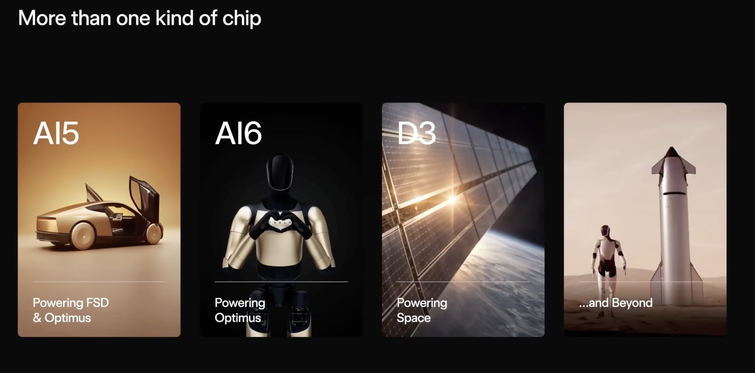
Image source: Terafab Terafab will produce two main types of chips
Reconstructing the Semiconductor Landscape and Facing Technical Challenges
While Musk’s plans are impressive, the semiconductor industry remains cautious about the technical feasibility. If Terafab starts with a 2-nanometer advanced process, it will face extremely high technical hurdles. Transitioning to GAAFET transistor architecture involves hundreds of complex, demanding steps, where even tiny deviations can cause yield failures.
TSMC’s long-standing process integration expertise and defect database form a strong technological moat. Additionally, the long lead times and high costs of advanced EUV lithography equipment, combined with the lack of mature semiconductor engineering talent and supply chain infrastructure in the U.S., are significant short-term obstacles.
Some industry observers see Musk’s announcement as a strategic move to demonstrate vertical integration capabilities, aiming to weaken the control of major foundries over their key customers. However, if Musk succeeds in integrating packaging technology and supply chain efficiency, he could, in the long run, reshape the global semiconductor power structure. This race for computing capacity, extending from Austin to outer space, is testing how this Silicon Valley maverick can turn science fiction into actual production capacity.
Disclaimer: The information on this page may come from third parties and does not represent the views or opinions of Gate. The content displayed on this page is for reference only and does not constitute any financial, investment, or legal advice. Gate does not guarantee the accuracy or completeness of the information and shall not be liable for any losses arising from the use of this information. Virtual asset investments carry high risks and are subject to significant price volatility. You may lose all of your invested principal. Please fully understand the relevant risks and make prudent decisions based on your own financial situation and risk tolerance. For details, please refer to
Disclaimer.
